As consumer demand for smaller yet more powerful mobile devices grow, manufacturers are turning to advanced packaging techniques to meet these requirements. One of the most promising innovations in this area is 3D packaging, which enables the stacking of multiple Integrated Circuits (ICs) vertically. This approach significantly enhances performance while minimizing the spatial footprint. Erik Hosler, a thought leader in mobile semiconductor innovations, recognizes that integrating 3D packaging in mobile devices is essential for balancing power efficiency with processing capability.
Mobile devices like smartphones, tablets and wearable technology continue to change rapidly. As users demand faster performance, longer battery life and more features, engineers face the challenge of packing greater functionality into increasingly compact designs. 3D packaging addresses this challenge by combining logic, memory and communication components into a unified stacked architecture.
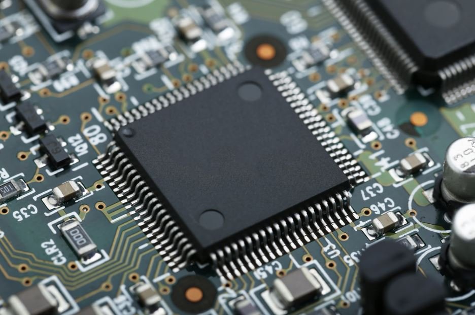
The Advantages of 3D Packaging in Mobile Devices
One of the primary advantages of 3D packaging in mobile devices is the ability to enhance processing power without increasing device size. By vertically stacking components, manufacturers can integrate more functionality within the same physical volume. It is particularly beneficial for high-performance mobile applications such as real-time video processing, gaming and Augmented Reality (AR).
3D packaging improves power efficiency by reducing signal transmission distances. Shorter interconnects between stacked dies lower resistance and decrease power loss. That means that mobile devices equipped with 3D integrated chips can maintain high processing speeds while consuming less energy.
Economic and Efficiency Gains
Adopting 3D packaging in mobile devices also offers economic advantages. By enhancing processing efficiency, manufacturers reduce the number of separate components needed, lowering production costs. More efficient designs also mean fewer failures and lower maintenance expenses over the device’s lifespan.
The compact nature of 3D integrated designs allows for more streamlined production processes. This efficiency helps manufacturers meet market demand for smaller, lighter devices while maintaining high performance. As mobile technology advances, companies that invest in 3D packaging will remain competitive by offering cutting-edge features without increasing production costs.
Addressing Heat Management Challenges
While 3D packaging offers numerous benefits, it also presents thermal management challenges. Stacking multiple ICs increases the risk of heat buildup, which can compromise device performance and longevity. To mitigate this, manufacturers are incorporating advanced cooling techniques such as microfluidic cooling channels and embedded heat spreaders.
Another approach involves using Phase-Change Materials (PCMs) that absorb excess heat during peak operation and release it as the device cools. This dynamic thermal regulation helps maintain optimal performance even during intensive processing tasks. Research into improved PCMs is ongoing, focusing on faster heat absorption and dissipation.
Advanced Thermal Management Techniques
To further improve heat management, manufacturers are exploring hybrid cooling systems that combine active and passive techniques. Embedding thin heat pipes within the chip stack helps distribute thermal loads while external cooling modules ensure heat dissipation from the device surface.
Thermal Interface Materials (TIMs) that incorporate high-conductivity elements like graphene are also being developed. These materials enhance the efficiency of heat transfer between stacked layers, reducing the risk of overheating during peak performance.
Enhancing Battery Life with Efficient 3D Integration
Power consumption is a critical consideration for mobile devices, where battery life directly impacts user experience. By integrating Power Management Units (PMUs) within the 3D package, manufacturers can optimize energy distribution and reduce waste. This approach not only extends battery life but also supports sustained performance during demanding applications.
The compact nature of 3D packaging reduces the need for separate power components, allowing for a more streamlined internal design. This results in lighter devices that do not sacrifice performance or battery longevity. As manufacturers continue to innovate, power optimization will remain a key focus.
Real-World Applications in the Mobile Industry
Leading smartphone manufacturers are already leveraging 3D packaging to enhance their flagship models. For instance, a major brand has integrated stacked memory and processing units to enable faster multitasking and smoother graphics rendering. This improvement directly contributes to enhanced user experiences in gaming and multimedia applications.
Wearable devices such as smartwatches are also benefiting from 3D integration. By stacking sensors, processors and communication modules, manufacturers can maintain compact designs without compromising functionality. This advancement is crucial for maintaining comfort and usability in wearable technology.
Sustainability Aspects of 3D Packaging
Incorporating 3D packaging in mobile devices supports sustainability by reducing material usage and energy consumption. Compact designs require fewer raw materials, which helps decrease environmental impact during manufacturing. Lower power consumption during device operation contributes to prolonged battery life, reducing electronic waste.
Manufacturers are also exploring the use of recyclable materials in 3D packaging to further reduce environmental impact. As sustainability becomes a central focus in consumer electronics companies that adopt eco-friendly packaging methods will gain a competitive edge.
Future Innovations in Mobile 3D Packaging
The integration of AI processing units within 3D packages is expected to improve mobile computing. By embedding AI accelerators directly within the chip stack, devices will be able to perform complex tasks like image recognition and voice processing with minimal latency.
The development of flexible 3D architectures could lead to foldable and wearable devices that adapt to user needs without sacrificing power. Researchers are exploring advanced materials like graphene to maintain structural integrity while enabling compact form factors.
The rapid advancement of mobile technologies requires continuous innovation in both hardware design and packaging techniques. Erik Hosler points out, “Modern society is built on CMOS technology, but as we push the boundaries of what these devices can do, we must innovate within the CMOS framework to continue driving performance efficiency and integration.” His perspective highlights the importance of leveraging advanced packaging to maximize mobile device capabilities without compromising on size or power.
Shaping the Future of Mobile Technology
3D packaging is proving to be pivotal in the mobile device industry. By enabling higher processing power, better battery efficiency and more compact designs, it addresses the core challenges of modern mobile technology. As manufacturers continue to innovate, integrating 3D packaging will become a standard practice for delivering next-generation mobile experiences.
Companies that embrace this technology will be better positioned to meet consumer expectations for faster, more efficient and feature-rich devices. As the mobile landscape changes, 3D packaging will play a key role in shaping the future of handheld and wearable electronics.